
In Pursuit of Low-Cost, Multifunctional, and Electrical Small Antennas for Microwave and Millimeter-Wave Communications
Prof. Ashwin K. Iyer
University of Alberta
20 July 2026
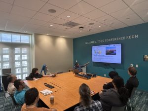
SDSU EIS-320 Conference Room
1500 – 1600
Attendance of 11 including speaker.
Dr. Satish Sharma (SDSU, and the organizer of the talk) introduced Dr. Iyer, describing his successful lab and shared connections with warmth and enthusiasm.
Dr. Iyer is fortunate to have the room to broadly explore antenna design topics in miniaturized microwave antennas. It was clearly evident from the presentation that his leadership is making an ongoing and enduring impact.
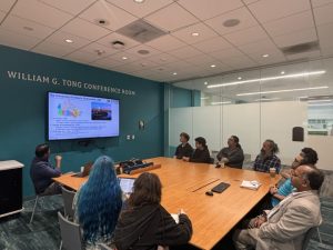
The talk covered many of the projects under consideration in his research group at the University of Alberta, located in Edmonton, the capital of the province. Located east of the Rockies, Edmonton is the most northern city in Canada with population of more than a million people and it serves as Canada’s primary logistical interface to the Arctic and boasts the continent’s largest stretch of continuous urban parkland. Research supporting tactical operations in the Arctic was a thread woven throughout the presentation.
The University of Alberta has over 46,000 students distributed among 18 faculties and generates 600 million in sponsored research revenue per year. It has a major open-access nanoFAB, which is free for use by students and open to industry to use as well. The ECE department has 60 faculty and is one of the largest ECE departments in Canada.
After this brief introduction, we had a pop quiz! Dr. Iyer showed two photos of people and asked “Who are they?” They were the bachelor’s graduation photos of George Sinclair, and Edward Jordan. George studied slot arrays, radar scattering, scale modeling. Edward researched antennas and radar, but is recognized for significant contributions to antenna education. Both were affected by their PhD advisor being absorbed by the US Signal Corps during WWII.
These two engineering researchers were pioneers in Canada, establishing antenna labs and attracting lots of researchers. Classical antenna science moved forward due to their efforts, and both Dr. Sharma and Dr. Iyer have connections their work.
The primary research theme of the lab is very low profile, weight, power, and cost antennas and microwave devices. “Low SWaPC” The lab focus includes the synthesis and modeling of denied EM environments. Antennas, sensors, meta-material devices for GPA, GPR, wires communications, security defense, and oil and gas are all considered. Defense work is a large part of the lab focus.
This means that the research concerns lots of sensors, antenna platforms, integrated platforms, zero-power biometric sensing, ad-hoc networks, meta-surfaces, signature management, and radar cross section. The lab partners with a variety of companies and organizations that those of us in the San Diego Section would be very familiar with.
The motivation is to innovate and refine electrically small antennas, meta-material-based antennas, and small antennas.
Challenges? There are clear challenges to this type of work. There are fundamental limits on bandwidth, quality factor, and gain. Matching impedances to the components and the environment is one of the most difficult challenges for very small antenna designs.
In order to get power radiated from even a very small antenna, you need a matching network. That matching network might be very bulky compared to the miniaturized antenna. If you do manage to get power into the antenna, the bandwidth ends up being small, because of losses exacerbated in the antenna. Small structures are difficult. Radiation efficiency is strongly reduced.
Dr. Iyer introduced an “Inherently Matched” electrically small folded dipole. Usually a half wavelength is the operating size/length of a dipole antenna. The resonance point was clearly shown on an impedance vs. length graph. Moving the resonance down, so that we get a smaller length, is the goal.
We reviewed inherent matching technique for Frequency Division Duplex Electrically Small Antennas (FDD ESAs). Dr. Iyer explained that the printed folded dipole with lumped L and C loading was used with positive results. This is a miniaturized planar folded dipole.
An Illuminating Contrast to ORI Work
A fully printed folded dipole looks very similar on the surface to Open Research Institute’s HF Dumbbell antenna, which uses a meander dipole structure at HF to dramatically reduce the physical size of a wire antenna while delivering high radiation resistance. Meander dipole miniaturization and tuning of planar printed dipole antennas clearly achieves high radiation efficiency while reducing size. Essentially, this is about min-maxing radiation efficiency vs. size, using meanders.
In traditional antenna miniaturization, engineers add physical, discrete components, such as a physical coil (inductor) or a physical capacitor (ceramic chip) to force a short antenna to resonate.
An HF or shortwave meander dipole antenna relies entirely on distributed (or parasitic) self-inductance and self-capacitance created inherently by its structural shape. The meander doesn’t radiate, but the remaining straight section of wire certainly does. At HF, the meander section is treated primarily as a delay line or a slow-wave structure rather than the primary source of the radio waves.
For the microwave structures that Dr. Iyer’s research group considers, the meander sections do radiate at microwave, but they do so in a highly asymmetric way that defines the polarization of the antenna.
Dr. Iyer’s Microwave Meander is a 2D structure on a dielectric substrate, perfect for integrating into miniaturized products. ORI’s HF antenna is a 2D Meander wrapped around a cylinder in order to create a sturdy structure that can be put up on a mast to get it high up enough to go on the air at the minimum HF antenna size.
Dr. Iyer’s microwave meanders act as the actual distributed radiator while compressing the physical length. At HF, ORI’s Dumbbell antenna acts as a non-radiating delay line to slow the wave speed down. Waves exit Dr. Iyer’s antennas broadly, including the meander section. At HF, ORI’s antennas see the waves exit in the straight wire sections, and not in the meander sections much at all.
At microwave frequencies, the tuning burden is on discrete components, instead of relying upon the physical meander structure of the antenna. This means that the meander is freed up to act purely as an efficient, compact, distributed radiator, allowing the antenna to maintain high radiation efficiency despite being much smaller than a conventional dipole.
The next example was a miniaturized RFID tag. Unbalanced currents on the feed, for small antennas, mean that the feed might end up radiating more than the antenna. To solve this clear and present danger to the utility of the antenna. Dr. Iyer’s group puts the RFID chip directly on the antenna. In other words, there is a conjugate match from the RFID chip directly to the antenna, in order to have the input impedance of the actual RFID chip be the target of the antenna match. There is no matching network, and therefore, no feed loss. Looking at the received signal strength, the quality of this match approach was confirmed. Essentially, this is abandoning the conviction that a 50 Ohm matching network must be between the RF signal output of the RFID chip, and the input electrical point of the antenna structure. The antenna matches whatever the RFID chip can produce, and then translates that to a “match” with free space.
The next example was an RFID-based temperature sensor, designed for free space or on-body applications. The on-board capacitor detunes antenna and temperature is detected. This ultra-miniature antenna has resonance frequency shifts across the RFID band that are correlated with temperature. The channel moves as the temperature changes the capacitor. This detunes the antenna. The 12 by 18 mm footprint is very small. The antenna geometry is designed for a conjugate match to the RFID chip impedance. The sensor radiates on the body, on the fingertips, and is designed to detect frostbite.
We then considered a concrete curing example. What if we included sensors in concrete? We would embed sensors for tracking the temperature and physical status. We can determine from the temperature profile how well a concrete structure has cured. The resonances are very narrow, and a fracture in the vicinity will shift the resonance. If the sensors last, then you can find failures over time.
Side note, Canada has an over the horizon radar project going on (30 feet high, 60 feet separation, over football field in width).
Dr. Iyer explained that traditionally, it has been mostly an ad-hoc process to miniaturize an antenna. He wanted to systematize the process, and he feels that they are making strong and consistent progress on this question.
Dr. Iyer changed gears from case studies and research projects to frame the Chu Limit, and what all this work means in terms of basic antenna theory. Antennas have a certain bandwidth capacity and quality factor. How low can it go for a certain size? This what the Chu limit addresses. The orginal research dates back to 1948 and involves circuit ladder networks, spherical wave expansions, and was done rigorously for the first few multipole orders, due to how grueling the computations were at the time. In 1964 Collins and Rothschild used field integration to confirm the Chu limit. However, Collins and Rothschild bypassed Chu’s circuit equivalents entirely when they did this. They calculated the stored energy by integrating the electromagnetic fields directly through space. While they arrived at values that mathematically matched Chu’s lower orders, a subtle and frustrating problem emerged in basic antenna theory. There was no universal, formal proof proving that Chu’s discrete equivalent circuit approach and Collins/Rothschild’s continuous field integration approach would always reconcile perfectly for an infinite number of higher-order multipole modes. It remained an unresolved, tricky gap in the fundamental literature.
So, Dr. Iyer’s lab united the theories and proved it with mathematical induction. What does this mean? The successfully bridged the two independent theories, which is a major contribution to the field. They proved that Chu’s ladder networks and the field integration models are dual expressions of the exact same physical reality across all arbitrary multipole orders, not just the first few. Mathematical induction really shines in this exact case, by taking a few successful solid results and extrapolating (correctly) to some larger or even infinite range of results.
By shifting the conversation from “how do we load this specific meander in this specific application” to “let’s mathematically unite the fundamental bounds of stored energy,” the research provides all of us engineers with an exact framework to evaluate exactly how close a highly miniaturized design (like the printed or cylindrical antennas discussed earlier) is to the absolute boundaries allowed by physics. This is delightful.
How does Dr. Iyer’s lab design optimal spherical miniature antennas? The optical geometry for spherical helical antennas can be predicted. Theory and results agreed for the structures that the lab tackled.
The next project was the leveraging of RFID to test small antennas. An achieved Ka, which is the dimensionless electrical size parameter, of 0.2 at 900 MHz, was presented and explained. Anything under 0.5 Ka is considered an electrically small antenna, so this is not a borderline result.
The reported Q of 198 or about 1.5x EP lower bound was then discussed. The quality factor Q inversely defines the antenna’s bandwidth. Because the antenna is tiny, its Q naturally skyrockets. The “EP lower bound” refers to the Elliptically Polarized lower bound. This is a stricter fundamental limit derived from spherical wave expansions. Achieving a Q of 198, which is only 1.5 times the absolute physical limit allowed by physics for that size, is an extraordinary design achievement indicating maximum possible bandwidth.
The particular antenna in this part of the presentation looks like a sake barrel with bifilar spherical helix arrangement wrapped around it. There is no feed network, as the RFID chip is directly connected to the antenna. Uniting the feed and the antenna is a key design pattern of the work in the lab.
This is one of several designs from Dr. Iyer’s lab where the traditional dipole arms are wrapped into a 3D spherical shell to maximize the utilization of the “Chu sphere” volume. “Bifilar” simply means it uses two symmetrically wrapped helical wire arms.
The slide presentation concluded and we went to Q&A.
Q: normally what is the level of power or gain that you usually get?
A: Close to the 1.5 dB limit. Which is much better than -13 dB that a lot of miniaturization ends up with. Usually it’s a horrible compromise between power and size.
Q: Can we use dispersion engineering to get multifunctional antennas and circuits?
A: Yes.
Dr. Iyer described how they designed a method of moments (MTM) based structure that is compact, uniplanar, fully printable, and included the full design procedure. This is a meta-material based electromagnetic bandgap structure MTM-EBG.
Coupled mode theory is used to produce a controllable bandgap. With a microstrip line, if you have two conductors, you have one mode.
So we can slot this structure and we can then produce something with, say, 4 conductors and therefore 3 modes. All TEM therefore they don’t couple. So, to force them to couple, we can make gaps and connect the conductors.
We load some conductors with capacitors and some with inductors. Phase might move backwards but the power always moves forwards.
The bandgap is created with coupled-mode dispersion. It can be printed. Printed gaps, printed conductors. Can you use this to build a multi-band antenna in one layer? Yes indeed. We “create two resonances for the price of one.”
Good operation was observed in both bands. Dual band and dual polarized patches were prototyped, at 3.6 Ghz and 5.8 GHz. They were fabricated and measured. They came in 1-1.4 dB lower than an equivalent patch antenna, but were much smaller.
Next, GPS/GNSS Antenna were shown, using a multi-layer MTM-EBG structure for the antenna design. This is a stacked patch antenna. Dr. Iyer’s lab collapsed it to a single patch, dual band at L1 and L2/L5. Solid PLA is the substrate. Extremely accurate due to the collapsed structure, on the order of 2mm resolution. Calian is the company that the lab is collaborating with, and commercialization of this antenna is expected in the next little while.
Dr. Iyer’s discussed the University of Alberta student cubesat project AlberatSat (launched twice). The project had turnstile rod antennas that mechanically deployed, but on the second launch they failed to deploy. Dr. Iyer’s lab proposed a flat antenna that has no moving mechanical parts? 437.5 MHz and S-band, patch antenna, instead of the turnstile rods.
Dual-band patch antenna design is 150mm by 86 by 6.35mm. It is mounted on the Nadir face, faces earth, and looks like it meets all their specs and will fly.
Drawbacks? It’s heavy. It’s like about a pound. To avoid the point of failure, the extra weight may be worth it. With and without the rails, with and without the cubesat package, was designed to be on the satellite.
Next up was a 20/30 GHz dual band. There are interior and exterior regions of the antenna. The gap sizes are 50 microns. This means very precise construction is required. Key aspect of this design is the ability to vary the polarizations and combinations of polarizations. This was achieved with chamfering the corners. It does produce the desired radiation characteristics. Physical prototypes showed port isolation larger than 25 dB.
How can we apply the MTM-EBG in other areas? Compact filters. Double-stub tuners. Stub matching networks. The lab is controlling the flow of current through the EBG regions. Uniplanar, three bands of matching. Capacitor and inductor going to ground, frequency dependent load, and designed for that load. Single port, complex impedance, chosen arbitrarily, so it can be redesigned for pretty much any load. Can be designed for three independent frequencies.
MTM-EBG based mechanically tunable filters were presented. Absolute bandwidth changes lowers with target frequency. But, what if we want consistent bandwidth? Filter is designed to maintain constant absolute bandwidth. Independently tune the three unit cells in the construction, and the problem is successfully addressed.
Next: Transmission line crossover. What about phased arrays? You have one PCB layer, but you want to operate in two different frequency bands. This is a challenging problem. Dr. Iyer showed a compact microwave filter for operation at 2.4 and 5.8 GHz. Like two train tracks that cross over each other.
Next was RFID-based real-time battery level monitoring, with a dual band antenna and diplexer system. Energy harvested in the field from 2.4 GHz enables communications over 915 MHz. Harvest to a battery, varactor across the battery. Modulate the impedance, backscatter communicate the battery level. Battery level goes up, varactor capacitance goes up, and the phase changes, and RFID backscatter indicates the voltage level on the battery. (see the OJAP special issue on antenna-enabled sensors and systems for more information about this particular design)
Dispersion Engineering is Fun
For meta-surfaces, can we use single sheets of flexible circuits to do wave front engineering? Yes we can. Waveguides and radomes are where this shows up.
We have flexible printed meander dipoles and we wrap this around a cylinder to where the pattern repeats.
This has a particular and interesting application in MRIs, where we change the frequency without requiring steep increases in the Tesla required of the magnets. You can fill the entire MRI with a dielectric, but those pesky patients kind of get in the way. The result of Dr. Iyer’s work is reduced risk of burns and better quality results without requiring big increases in Tesla.
Another case study is sectorized antennas for cellular phones. These sectors have seams. The seams are not perfect. There’s different ways to address this. Overlap the sectors, or rework the antenna, or use meta surfaces in radomes in order to change the pattern and reduce the impact of the seams. Placed over the antenna array, the material modifies the gain pattern. The dual use of this is signature management, to change the characteristics of an antenna in the field to avoid detection.
Q: What is the size of the GPS Antenna?
A: 80mm or so
Q: What do you use for antenna modeling?
A: Mainly HFSS, FICO, CST
Dr. Iyer closes with describing and emphasizing the value of a teacher and teaching in general. Doing things with a certain level of integrity, whether you are teaching in the literal sense, or doing something for the benefit of others, the quality and values of your advisor is key. Dr. Satish Sharma highlighted Dr. Iyer’s quality of work and teaching excellence.
Dr. Satish explained that SDSU has offered a lot of master’s level work to students, traditionally. Over the years, it’s grown and developed into better research environment for PhD work. Now there is a joint PhD program with UCSD, for example. However, some students want to just get the degree and get out. That is ok, because they are on a self-assigned mission, or see a need that needs to be filled somewhere in the world and they are drawn to it. Some students are at University to learn and study deeply, and make a real difference within the research lab or setting. SDSU accepts undergraduates and masters students in research, in contrast to some other universities. A quote from this discussion was “there’s no magic line between a MS and PhD student. They both have the potential to achieve great things and have fulfilling experiences”
Dr. Iyer testified that teaching is a very fulfilling experience and can be done in or outside of the classroom. Antenna engineers have to visualize everything that they are doing. We cannot see electromagnetic waves. In Dr. Iyer’s view, people in electromagnetics tend to be exceptional teachers because of the intensity of the necessity of visualization. It’s more important to remember learning how to think and not necessarily about retaining all the tiny details.
After the presentation, attendees enjoyed some refreshments at Starbucks and then took a group photo.

Thank you to Dr. Satish Sharma for organizing a deeply meaningful afternoon for antenna and propagation enthusiasts.